
US chipmaker Onsemi has unveiled its Embedded Power Platform (EPP), a new chip architecture that increases power density in AI data centers and other high-power applications.
The platform uses the silicon wafer as an embedded package, integrating electrical, mechanical, and thermal design to allow customers to achieve a higher power density and improve AI system performance.

Speaking to DCD ahead of the announcement, Dinesh Ramanathan, SVP of corporate strategy at Onsemi, explained that racks today are roughly 60kW, but in the next two years that is expected to rise to 200kW, hitting 1MW by the end of the decade.
“The space in the rack isn't changing, but the amount of power that rack is going to end up consuming is increasing by a dramatic amount,” Ramanathan said. “So, if you have to support that and make sure that data center rack can consume the 1MW and give us the kind of AI capabilities that we're looking for, then we have to drive towards an increase in power density across that entire rack. If we can't increase the power density across the entire rack, we'll never be able to reach 1MW.”
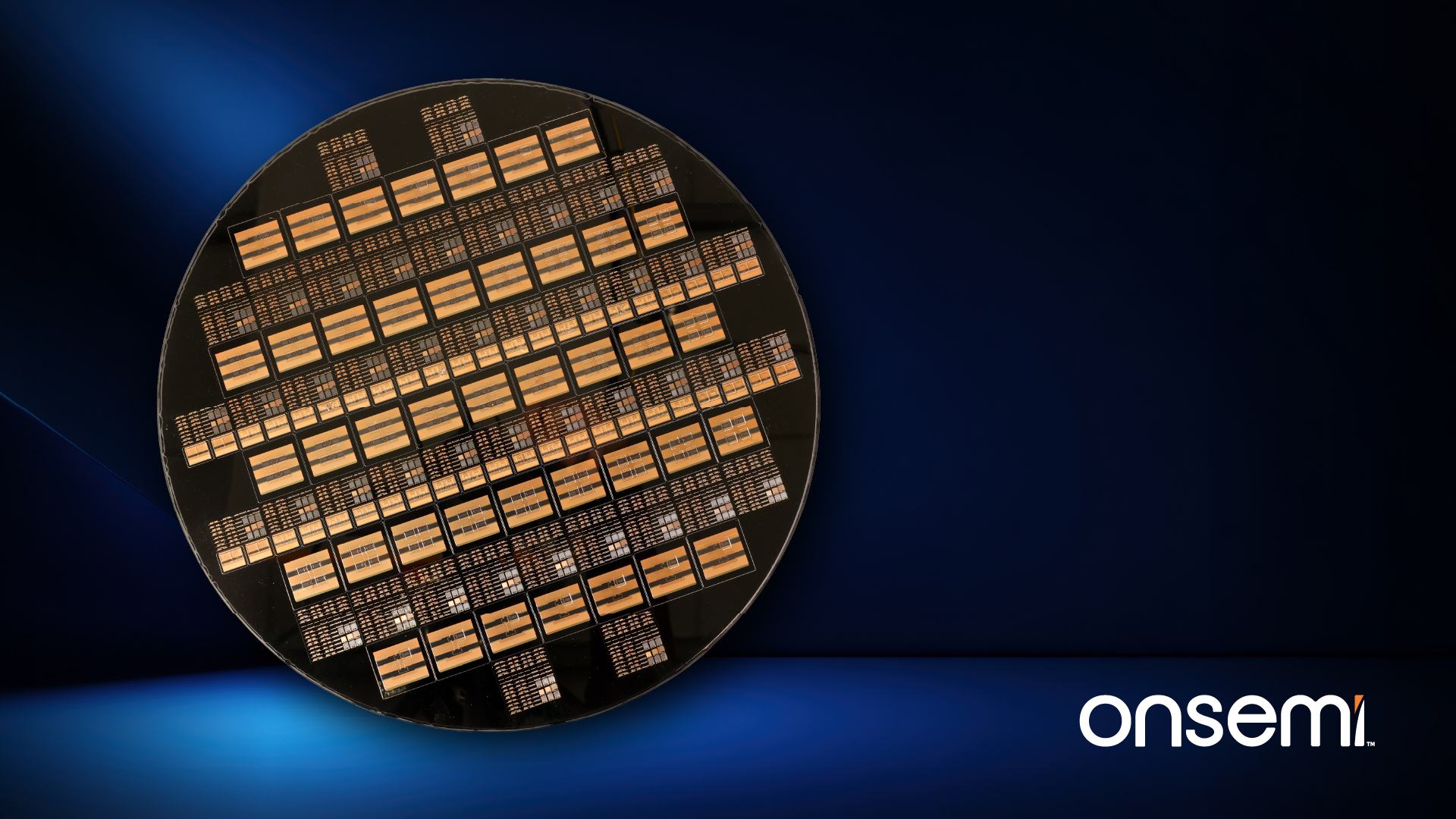
Ramanathan explained that on a basic level, EPP works by taking a silicon wafer, making a cavity inside it, and then taking the die and putting it into the cavity. By using the wafer as the package, silicon, silicon carbide, and vertical gallium nitride can then be “seamlessly” interconnected within a “highly integrated wafer-level architecture.”
The platform also allows multiple devices, including FETs, drivers, and controllers, to be embedded together in a single package that has been co-optimized for electrical, thermal, and mechanical performance. According to the company, in an early EPP-based solid-state circuit-breaker design, the solution was found to be approximately 50 percent smaller and 20 percent cooler than existing designs.
EPP leverages Onsemi’s standard 12-inch silicon wafer manufacturing capabilities, including mature semiconductor design tools, wafer-level manufacturing, advanced simulation capabilities, and power system integration.
“By reducing packaging overhead and using the full EPP footprint to conduct heat, EPP can support more compact power systems, improve thermal management and enable greater power density in AI infrastructure,” the company said in a statement.
Onsemi has already partnered with Subaru for the deployment of EPP, with the company set to gain early access to engineering samples, simulation models, and technical expertise. Ramanathan said the chipmaker was also partnering with both an industrial and AI data center company, although he said Onsemi was not currently in a position to name them.
“We have shown [these customers] what the technology can do, and we're working towards getting this product into revenue in the 2027 time frame, so we're sampling our customers this year,” Ramanathan said. “The expectation is that in Q1, this technology will be qualified, and then made generally available for any of our customers to take to market.”





Comments