Lightmatter has unveiled two new photonic interconnect solutions designed to tackle the bandwidth challenges associated with increasingly dense AI deployments.
Dubbed the Passage M1000 and the Passage L200, both offerings will integrate with next-generation XPUs and switches.
Boston-based Lightmatter specializes in photonics-enabled technologies that use light instead of electrical signals for computing, meaning its chips don’t experience the same heat or resistance as traditional chip architectures. The new solutions have been built on the company’s Passage interconnect technology, a chip that takes arrays of traditional processors and links them up using a programmable on-chip optical network.
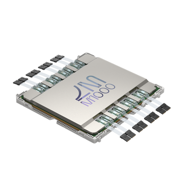
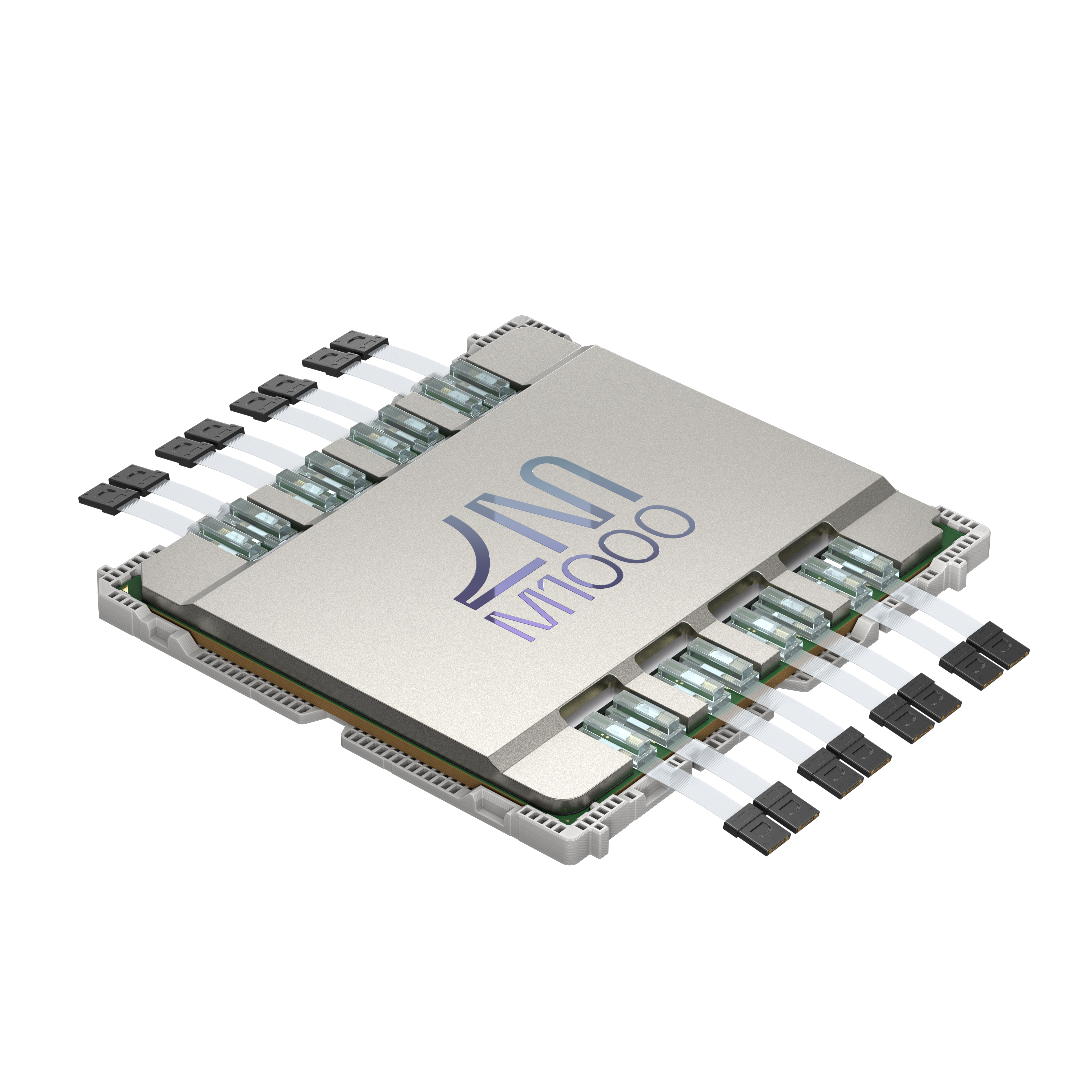
According to Lightmatter, the M1000 enables a “record-breaking 114Tbps total optical bandwidth for the most demanding AI infrastructure applications,” providing connectivity to thousands of GPUs in a single domain.
Consisting of an eight-tile 3D interposer with an integrated programmable waveguide network, the M1000 also contains 3D integrated electrical integrated circuits containing a total of 1024 Electrical SerDes (Serializer/Deserializer - technology which is used to reduce the number of inputs and outputs on an ASIC or FPGA), 56Gbps NRZ modulation, and eight wavelength WDM transmission on waveguides and fibers.
The offering also has 256 optical fibers edge attached with 448Gbps bandwidth per fiber and delivers 1.5kW of power in an integrated advanced package.
Due to be available from summer 2025, the M1000 will be produced by GlobalFoundries and Amkor and utilize GF Fotonix, a silicon photonics platform that integrates photonic components with CMOS logic into a single die.
“Passage M1000 is a breakthrough achievement in photonics and semiconductor packaging for AI infrastructure,” said Nick Harris, founder and CEO of Lightmatter. “We are delivering a cutting-edge photonics roadmap years ahead of industry projections. Shoreline is no longer a limitation for I/O. This is all made possible by our close co-engineering with leading foundry and assembly partners and our supply chain ecosystem.”
Meanwhile, Lightmatter also announced its upcoming 3D photonic L200 interconnect.
Described as the world’s “first 3D co-packaged optics (CPO) product,” the L200 3D CPO product portfolio consists of the 34Tbps L200 and the 64 Tbps L200X, which the company claims will enable more than 200Tbps of total I/O bandwidth per chip package, resulting in up to 8x faster training time for advanced AI models.
The solutions will also use a standard interoperable UCIe die-to-die (D2D) interface, which Lightmatter said will facilitate “scalable chiplet-based architectures to seamlessly integrate with next-generation XPUs and switches.”
The Passage L200 integrates with Alphawave Semi’s latest chiplet technology portfolio, with Alphawave offering the IP for the accompanying XPU/Switch die royalty-free.
Due to be available in 2026, the L200 will be manufactured in partnership with GlobalFoundries, ASE, Amkor, and advanced node CMOS foundries.


