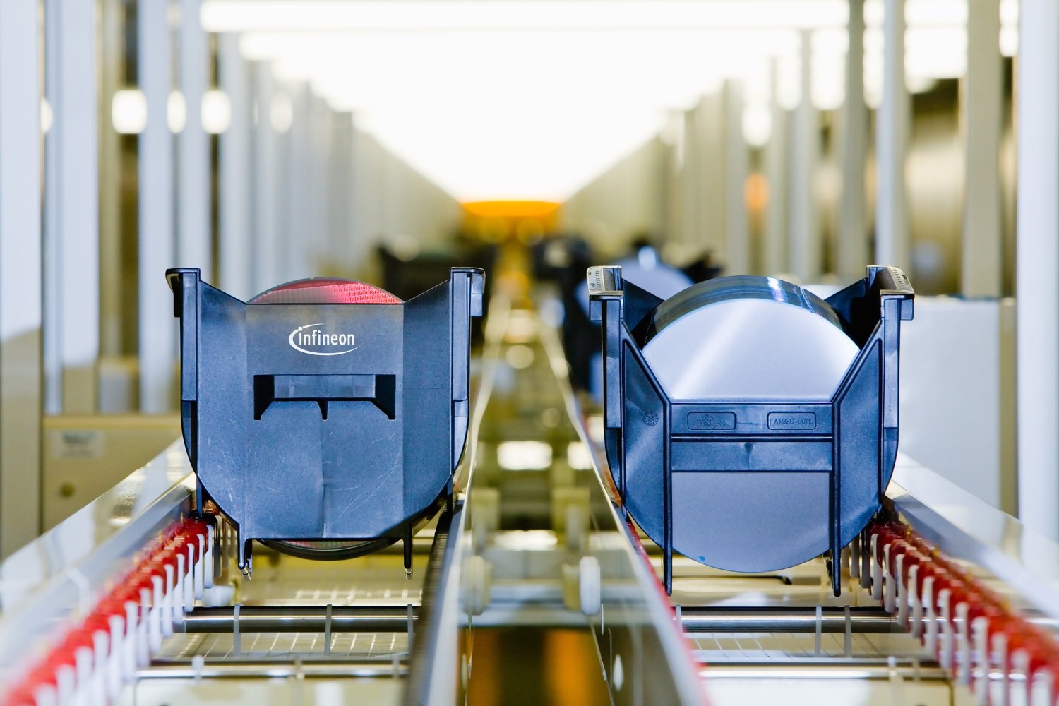
The European Commission (EC) has approved a €920 million ($964m) funding package to support the construction of Infineon’s new chip fab in Dresden, Germany.
The funding will allow the German chipmaker to complete its so-called MEGAFAB-DD project. The company has said it will produce both discrete power technologies and analog/mixed-signal integrated circuits at the facility.

In a statement, the EC said the fabrication plant will be the first in Europe to be able to rapidly switch production between the two technology families while maintaining high output capacity. The front-end facility will offer wafer processing, testing, and separation capabilities and is expected to be operating at full capacity by 2031.
In total, Infineon is expected to invest approximately €3.5 billion ($3.7bn) in the project. The funding from the commission is part of a larger €15bn ($15.8bn) funding pot established by the EC to support both public and private semiconductor initiatives.
"The €920 million German measure approved today supports a cutting-edge megafab in Dresden,” said Teresa Ribera, EVP for clean, just, and competitive transition at the EC. “This project will support the development of a strong and resilient digital economy in Europe and ensure a secure supply of semiconductors for the industry while limiting any potential distortion of competition.”
In addition to the MEGAFAB-DD project, Infineon has a 10 percent stake in TSMC’s ESMC (European Semiconductor Manufacturing Company) facility, also in Dresden. The plant is due to be operational in 2027 and, when complete, will produce 40,000 wafers a month.
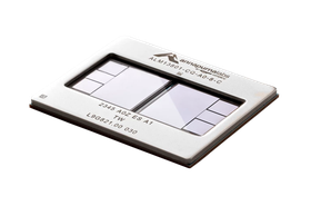
In October 2024, Infineon unveiled the world’s thinnest silicon power wafers, with a thickness of 20 micrometers and a diameter of 300 millimeters. The company said the wafers are half as thick as current state-of-the-art wafers, which measure between 40-60 micrometers. One millimeter is the equivalent of 1,000 micrometers.
That announcement comes less than two months after the German chipmaker announced it had successfully developed the world’s first 300mm power gallium nitride (GaN) wafers.


