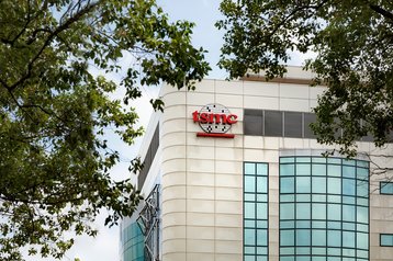
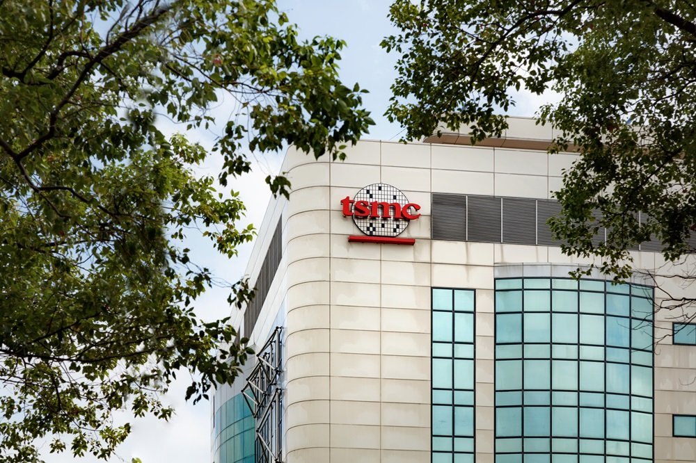
Chipmaker TSMC is partnering with Ansys, Synopsys, and Cadence to develop its silicon photonics integration system capabilities.
Engineering simulation software firm Ansys and TSMC are collaborating on the chipmaker’s Compact Universal Photonic Engine (COUPE) silicon photonics integration system.
Chip design tool provider Synopsys is helping the company optimize photonic integrated circuit (PIC) flow.
The collaboration with Cadence will extend a long-standing partnership between the two companies that has resulted in the development of 3D integrated chips and advanced process nodes to design intellectual property and photonics.
TSMC initially unveiled its silicon photonics program at its 2024 North American Technology Symposium in late April. This event saw the company lay out its plans to improve on-package connectivity by eventually bringing 12.8Tbps of optical connectivity to TSMC-made processors.
To achieve this aim, TSMC is developing COUPE technology which uses SoIC-X (System on Integrated Chips) chip packaging technology to stack a 65nm electronic integrated circuit (EIC) on a PIC. TSMC says this technique offers the lowest impedance at the die-to-die interface and therefore improves energy efficiency.
Silicon photonics has long been touted as a solution to help data centers deal with increasing bandwidth demands and improve connectivity between servers and switches. The technology involves using silicon instead of glass as the light-transport medium to create photonic integrated circuits.
The development of TSMC’s COUPE technology will span three phases. In 2025, TSMC plans to produce an optical engine for OSFP (Octal Small Form Factor Pluggable) connectors, enabling a data transfer rate of 1.6Tbps.
The following year, the company will integrate COUPE into CoWoS (Chip on Wafer on Silicon) packaging as co-packaged optics – the advanced heterogeneous integration of optics and silicon onto a single packaged substrate – with a switch, enabling motherboard-level optical interconnections with speeds of up to 6.4Tbps.
The final phase is designed to be integrated into processor packaging, which TSMC is hoping will produce data transfer rates of up to 12.8Tbps. No release timeline has been provided for this final phase.
“We are entering an AI-empowered world, where artificial intelligence not only runs in data centers, but PCs, mobile devices, automobiles, and even the Internet of Things,” said TSMC CEO C.C. Wei.
“At TSMC, we are offering our customers the most comprehensive set of technologies to realize their visions for AI, from the world’s most advanced silicon, to the broadest portfolio of advanced packaging and 3D IC platforms, to specialty technologies that integrate the digital world with the real world,” he said.
Other new technologies TSMC announced it was focusing on at April’s Technology Symposium include A16 technology to improve chip density for data center products; NanoFlex technology which will allow chip designers to mix and match cells from different libraries within the same block design; a newly optimized 5nm-class node called N4C; the development of CoWoS, SoIC, and TSMC-SoW (System-on-Wafer) technology; and automotive advanced packaging.
